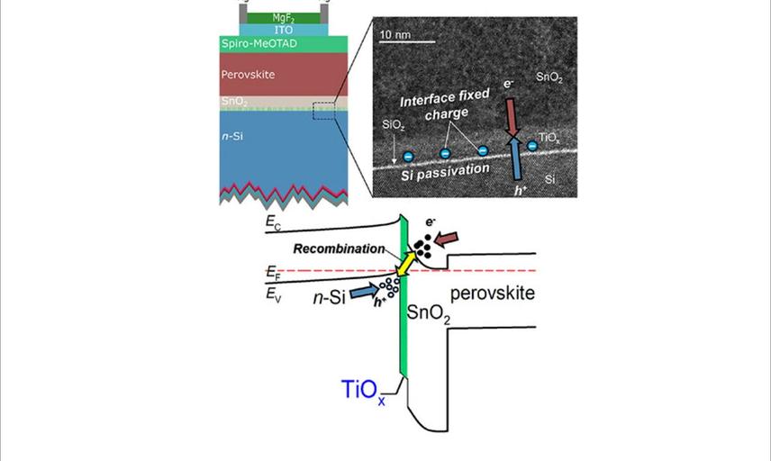
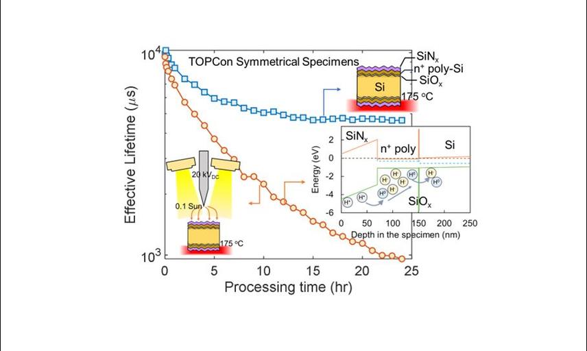
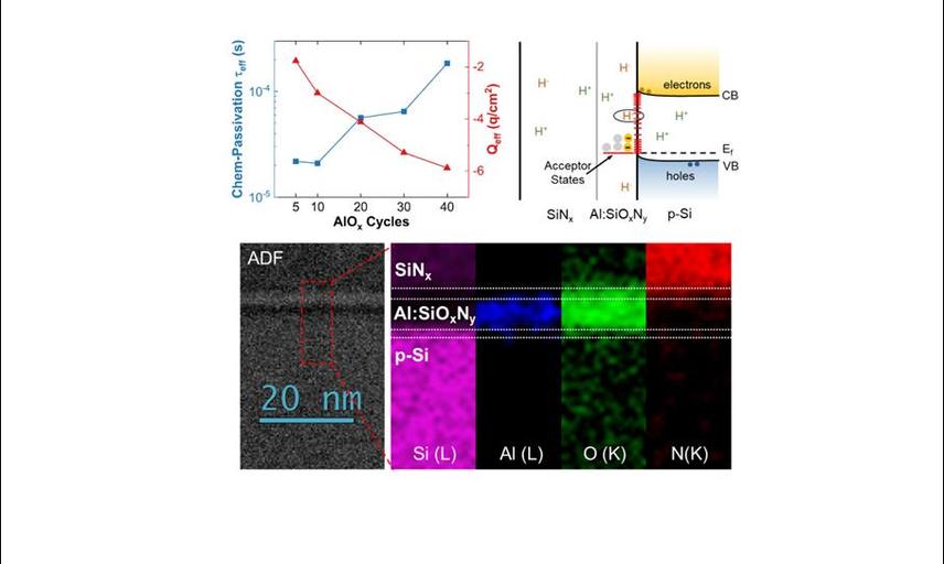
Solar Energy Materials and Solar Cells, Vol 282, 2025. TOPCon silicon solar cells, known for their high performance, can lose performance due surface-related degradation (SRD). Cells can become unstable after high-temperature processes during manufacturing, leading to reduced performance. When an electric field is present on the cell's surface, it accelerates degradation. This is because hydrogen ions within the cell, which are essential for its function, migrate under the electric field, creating defects at the cell's surface.